
Date of Publish: 14/04/2026
Stock Price: 764.60 EUR
ASM International: Equity Research Report
Company Overview
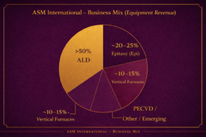
ASM International is a semiconductor wafer fabrication equipment (WFE) company based in Amsterdam, specialising in deposition technologies. Its primary focus is Atomic Layer Deposition (ALD), which accounts for more than 50% of revenue and represents the core driver of business growth. The company also operates in secondary segments including epitaxy (Epi), vertical furnaces, PECVD, and silicon carbide (SiC) epitaxy. However, ALD clearly forms the foundation of the business, with ASM holding a leading position in this niche process and an estimated global market share of over 55%.
Value Chain Positioning
The semiconductor value chain can be broadly broken down into three key segments:
- Designers – companies such as NVIDIA
- Foundries / IDMs – including TSMC, Intel, and Samsung
- Equipment suppliers – where ASM International operates
ASM’s role within the value chain is to supply the tools used in wafer fabrication, specifically enabling the deposition of materials at the atomic scale. This positioning detaches ASM from direct exposure to end-demand for chips and instead aligns it more closely with semiconductor capital expenditure cycles.
Core Technologies
Atomic Layer Deposition (ALD)
ALD is a highly precise thin-film deposition technique used in semiconductor manufacturing to build material layers one atomic layer at a time. Through sequential, self-limiting chemical reactions, it enables exceptional uniformity, conformal coating over complex 3D structures, and atomic-level thickness control. This makes it essential for producing high-performance, compact semiconductor devices and is the core contributor to ASM’s revenue.
Epitaxy (Epi)
Epitaxy is a process used to grow thin, high-purity crystalline layers on a substrate while maintaining its atomic structure. This is critical for forming advanced transistor and memory architectures, allowing precise control of electrical properties and material composition. Epi represents ASM’s second-largest revenue segment and an important area of future growth.
Supporting technologies
Additional processes such as vertical furnaces (batch processing), PECVD (complementary deposition), and SiC epitaxy (power electronics applications)
exposure to both mature and emerging semiconductor applications make up the remainder of ASM’s product portfolio, providing
Industry Structure
ASM operates in the Wafer Fabrication Equipment (WFE) industry, where companies manufacture the tools and machines used in semiconductor production. Key process steps include lithography, deposition, etch, and metrology.
As mentioned previously, ASM’s primary focus is the deposition process. Deposition is the step in semiconductor manufacturing where material layers are added to the wafer, meaning it directly defines device structure and electrical performance. ASM’s focus on atomic-scale deposition, particularly through ALD, places it in one of the most precision-sensitive and yield-critical stages of the process flow.
Within WFE, competition occurs at the level of individual process steps rather than across the full manufacturing process. ASM is not a broad WFE provider, but instead operates primarily within deposition, with a particular focus on Atomic Layer Deposition (ALD) as its core segment and epitaxy (Epi) as a secondary area. This narrower positioning distinguishes ASM from more diversified equipment peers and places it in a specialised segment of the market.
Industry Relevance
Historically, semiconductor scaling was primarily driven by lithography, enabling smaller transistors through improved patterning. However, as devices approach physical limits related to leakage, heat, and variability, scaling is increasingly dependent on materials engineering. Performance is now driven by what materials are used, how precisely they are deposited, and how interfaces behave at the atomic level.
Atomic Layer Deposition plays a central role in this shift. By enabling material layers to be built one atomic layer at a time, ALD allows for precise thickness control, conformality across complex 3D structures, and the integration of new materials. As devices transition from planar designs to nanoscale 3D architectures, traditional deposition methods become insufficient, making ALD not just preferred but necessary.
This transition is being driven by key technology inflections such as gate-all-around (GAA) transistors, advanced DRAM, and 3D NAND. These technologies significantly increase both the number and precision of material layers required in each device, directly increasing the number of deposition steps per wafer, particularly for ALD and epitaxy. This is particularly evident in leading-edge nodes, where the number of ALD layers per device has increased materially, with management highlighting a continued rise in ALD intensity at each successive node.
ASM’s economic model is structurally leveraged to this increase in device complexity. While many semiconductor companies are primarily driven by unit demand and therefore subject to strong cyclicality, ASM’s revenue is increasingly driven by both wafer volumes and the number of process steps per wafer. As device complexity increases, so too does the number of ALD and Epi steps required, structurally expanding ASM’s addressable market.
The number of ALD and Epi steps per wafer is increasing with each technology node, meaning deposition intensity is growing faster than overall semiconductor unit demand. While the WFE market is inherently cyclical, the increasing importance of deposition, particularly ALD, creates a structurally growing and economically attractive segment in which ASM is highly concentrated. With a leading position in ALD and a growing presence in epitaxy, ASM is well positioned to benefit from both cyclical recovery in semiconductor capex and long-term structural growth driven by increasing materials complexity.
Competitive Structure
The WFE market is highly concentrated, with a small number of scaled players dominating individual process steps. While ASM operates as a specialist in deposition, particularly ALD, its competitive positioning is best understood relative to broader WFE peers with varying degrees of process coverage and scale.
Applied Materials is the broadest and most diversified competitor within WFE. The company operates across multiple process steps, including deposition, etch, inspection, and packaging-related technologies, and emphasises an integrated “materials engineering” approach. While Applied does compete directly with ASM in deposition, its strength lies in scale, breadth, and its ability to integrate solutions across the manufacturing process. As a result, deposition represents a meaningful but minority portion of its overall business, with ALD forming only one part of a broader deposition portfolio rather than a core strategic focus.
Lam Research is more focused than Applied but is primarily concentrated in etch and clean processes, where it holds leading market positions. The company also participates in deposition, though this is not its core strength. Lam’s positioning provides a useful contrast, as it is more exposed to adjacent process steps and to memory markets, which tend to exhibit higher cyclicality. While it has ALD capabilities, these are not a central driver of its competitive positioning.
Tokyo Electron operates as a broad WFE provider with strong positions across deposition, etch, and cleaning, as well as lithography track systems. The company has a particularly strong footprint in Asia and benefits from close relationships with leading foundries. Tokyo Electron competes with ASM in deposition, including ALD, but its exposure is spread across multiple process steps and does not exhibit the same level of concentration in advanced ALD technologies.
Across these peers, a clear distinction emerges between breadth and specialisation. Applied Materials and Tokyo Electron operate with broad process coverage, leveraging scale, integrated solutions, and large installed bases, while Lam Research is more focused but remains centred on adjacent process steps. In contrast, ASM is significantly more specialised, with a concentrated focus on deposition, particularly ALD and epitaxy. This narrower positioning limits its exposure to the full WFE stack but allows it to compete more directly on process performance in highly technical and increasingly critical steps of semiconductor manufacturing.
While multiple WFE players participate in ALD, ASM’s position within the segment is structurally differentiated. The company holds an estimated market share of over 55%, with the remainder fragmented across competitors such as Applied Materials and Tokyo Electron. However, this competition is not evenly distributed across all ALD applications. ASM is particularly dominant in single-wafer ALD at advanced nodes, where precision requirements, conformality, and atomic-level control are most critical. In contrast, competitors tend to have broader but less concentrated exposure, often spanning multiple deposition technologies or focusing more heavily on batch processing and adjacent process steps.
As a result, while ASM is not the only company operating in ALD, it is uniquely positioned in terms of both scale and specialisation within the highest-value segment of the market. Its leadership is not simply a function of overall ALD share, but of its concentration in the most technically demanding and economically attractive applications, where barriers to entry, qualification requirements, and process sensitivity are highest.
A useful comparison can be drawn between ASM’s position in ALD and ASML’s position in lithography, though the strength of that comparison has limits. In lithography, ASML holds a near-monopolistic position, particularly in EUV, where it is effectively the sole supplier of leading-edge tools. In contrast, while ASM holds a leading share of over 55% in ALD and is particularly dominant in single-wafer ALD at advanced nodes, the market remains competitive. The parallel lies less in market structure and more in strategic importance, as both lithography and advanced deposition are critical enabling steps where performance, yield, and scaling are highly sensitive to process precision. As a result, both occupy areas of the value chain characterised by high barriers to entry, deep customer integration, and strong pricing power, though ASM operates in a more competitive environment where its advantage is driven by technological leadership and specialisation rather than outright market control.
Industry Economics
Unlike other sections of the semiconductor value chain, this is not a commoditised industry. Returns are structurally high, but not evenly distributed. WFE tools are mission-critical for producers, and their performance directly affects yield. As a result, pricing power exists within the market, with value accruing in the most process-critical and hardest-to-replace steps.
Switching Costs
WFE tools are deeply embedded within process flows, and changing vendor can pose a significant risk to production. This level of complexity leads customers to avoid switching suppliers, allowing WFE companies to retain pricing power and benefit from higher revenue stability. For ASM, processes such as ALD require an extremely high level of precision, resulting in even greater switching costs.
Qualification Cycles
Due to strict industry standards, tools must be tested and approved before being deployed in production. This process requires significant time, cost, and engineering effort. These barriers make entry difficult for new competitors and provide structural protection for incumbents. This dynamic is further amplified in the case of ASM, where the complexity of ALD tools makes qualification even more demanding.
Yield Sensitivity
Yield refers to the percentage of functional chips produced. In such a complex, multi-step manufacturing process, even small changes can have large impacts, including yield loss, delays, and supply disruptions. As a result, customers prioritise reliability over price, reinforcing pricing power and supporting margins. With ALD operating at the atomic level, it is one of the most yield-sensitive steps, and customers are willing to pay a premium to ensure consistency and performance.
IP and Process Know-how
Value in this industry does not lie solely in the hardware, but also in the underlying materials science and process expertise. This intellectual property is difficult to replicate and requires long, capital-intensive R&D cycles. As one of the most knowledge-intensive steps in semiconductor manufacturing, ALD further strengthens this dynamic for ASM.
Installed Base and Recurring Revenue
Once a tool is installed, revenue continues through service, spare parts, and upgrades. This creates a recurring revenue stream that supports higher margins, improves revenue visibility, and increases customer lock-in over time.
Market Concentration
The WFE market is highly concentrated, with a small number of major players dominating each process step, resulting in an oligopolistic structure. Companies such as Applied Materials, Lam Research, and Tokyo Electron operate across multiple process steps, while ASM remains primarily focused on deposition, particularly ALD and epitaxy. This combination of concentration and specialisation further limits competitive pressure and supports sustained returns.
Conclusion
The WFE market is characterised by high barriers to entry, strong customer lock-in, and an oligopolistic structure, resulting in structurally attractive economics. However, value does not accrue evenly across all process steps. The highest returns are concentrated in areas that are most sensitive to yield, most difficult to qualify, and most critical to device performance. Deposition, and particularly ALD, sits firmly within this category due to its role in defining material structure at the atomic level. As semiconductor architectures continue to increase in complexity, these characteristics become more pronounced, further reinforcing the importance of advanced deposition. As a result, ASM is not only positioned within a structurally attractive industry, but within one of its most economically advantaged segments, where increasing process intensity, strong pricing power, and high switching costs support long-term value creation.
Key Drivers
In this section, I will analyse the five main drivers I have identified that are expected to support ASM International’s growth and returns over the coming years.
Driver 1: GAA Transition
What is changing
The semiconductor industry is transitioning from FinFET to Gate-All-Around (GAA) architectures at the 2nm node and below. GAA introduces nanosheet transistors, which are fully 3D structures. These require:
- More work-function metals
- More dipole layers
- Tighter interface control
All of these are ALD-intensive layers where atomic precision is required. Epitaxy (Epi) also becomes critical for channel formation within the nanosheets, as well as for material purity and strain engineering.
Why ASM benefits
As the market leader in single-wafer ALD, ASM is strongly positioned in the front-end transistor stack, which represents the highest value portion of the device. In addition, the company is increasing its Epi share within leading-edge logic, further expanding its exposure to these layers.
Trend Evidence
ASM expects its served available market (SAM) to increase by approximately $400m in the transition from FinFET to first-generation GAA, with a further $450–500m expansion expected at 1.4nm.
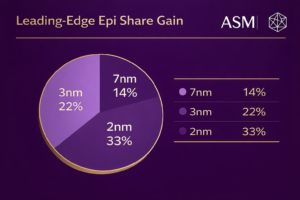
Epi share within the process is expected to increase from 22% to 33%, while transistor-related ALD layers rise from 50% to 60% by 1.4nm.
Key Insight
This transition is not linear. ASM is not simply participating in node transitions, but capturing a disproportionate share of process wallet expansion per node.
Conviction: High
Driver 2: DRAM / HBM / Memory Inflection
What is changing
AI expansion is driving heightened demand for High Bandwidth Memory (HBM) and advanced DRAM scaling. HBM requires high-k metal gate ALD and highly precise dielectric layers.
Looking forward, the DRAM roadmap includes a transition to 4F² architecture, introducing more 3D structures and increasingly “logic-like” process steps.
Why ASM benefits
These changes increase the number of ALD layers per memory cell and introduce incremental Epi adoption in memory. With a strong position in high-k ALD and growing exposure to Epi, ASM is well positioned to benefit. Importantly, this expands ASM’s exposure beyond logic into a second major segment.
Evidence
Memory exposure has increased significantly, rising from 11% of equipment sales in 2023 to 25% in 2024, driven primarily by HBM-related demand.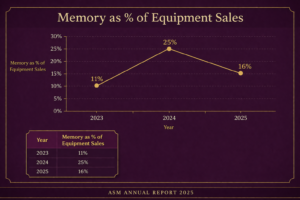 The transition to 4F² is expected to further increase ALD and Epi intensity per device.
Key Insight
While ASM is often viewed as a logic-driven company, memory is increasingly becoming a second structural growth engine, rather than a purely cyclical contributor.
Conviction: Medium–High (structural trend with cyclical overlay)
Driver 3: ALD Intensity per Device (Structural Growth Trend)
What is changing
Scaling in the semiconductor industry is no longer primarily driven by shrinking dimensions, but by materials engineering. Devices now require more interfaces, material stacks, and 3D structures to improve performance and power efficiency.
ALD is critical in enabling this, as each new node adds layers rather than simply reducing size.
Why ASM benefits
With a dominant position in advanced-node ALD, particularly in the front-end transistor stack, ASM is directly exposed to increasing process complexity. This is a highly specialised segment with significant barriers to entry.
Evidence
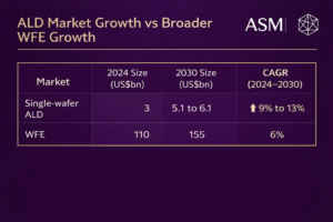
ASM continues to report increasing ALD layer counts at each successive node. The ALD market is expected to grow at 10–14% CAGR, compared to 5–7% for the broader WFE market.
Key Insight
ASM’s growth is not purely volume-driven. While wafer volumes remain cyclical, increasing process intensity per wafer provides a structural growth driver independent of volume.
Conviction: Very High
Driver 4: Epi Share Gains
What is changing
Epitaxy is becoming increasingly important in GAA nanosheet formation, advanced material stacks, and future DRAM architectures. These applications require high-quality crystalline growth and atomic-level control, increasing Epi’s share of device-defining layers.
Why ASM benefits
ASM has been gaining share in leading-edge Epi and is able to leverage its existing ALD relationships to drive further adoption and integration.
Evidence
ASM has increased its leading-edge Epi market share from approximately 12% in 2020 to 25% in recent years, with a target of ≥30%.
Key Insight
While ALD represents ASM’s core moat, Epi provides an incremental share-of-wallet expansion lever, particularly at advanced nodes.
Conviction: Medium (execution dependent but strong trajectory)
Driver 5: Spares, Services & Advanced Packaging (Combined)
What is changing
ASM’s installed base of tools continues to grow, increasing demand for spares, maintenance, and upgrades. At the same time, the company is expanding into outcome-based services and exploring adjacent opportunities such as advanced packaging.
Why ASM benefits
A larger installed base drives recurring service revenue, which is typically more stable and higher margin. In parallel, advanced packaging represents a longer-term growth opportunity aligned with ASM’s strengths in materials engineering and interface control.
Evidence
Spares and services revenue has grown at approximately 19% CAGR between 2020 and 2024, with continued double-digit growth expected going forward.
Advanced packaging remains an active R&D focus with expected contribution over the coming years.
Key Insight
Services provide downcycle resilience and margin stability, while advanced packaging represents a credible but non-core growth option.
Conviction: High (services) / Low–Medium (advanced packaging)
Conclusion
ASM’s growth profile is driven by a combination of structural and cyclical factors, but the key differentiator lies in its exposure to increasing device complexity rather than simply semiconductor unit demand. As scaling shifts from lithography to materials engineering, the number and importance of deposition steps continue to rise, structurally expanding ASM’s addressable market.
This positions the company to benefit disproportionately from major technology inflections such as GAA and advanced DRAM, while additional upside is provided through Epi share gains and a growing recurring service base. As a result, ASM is not just levered to semiconductor growth, but to the most complex, highest-value, and fastest-growing parts of the manufacturing process.
Financials
Revenue
ASM’s revenue performance reflects a business increasingly detached from pure cyclicality and instead driven by structural growth. Revenue increased from €2.6bn in 2023 to €2.9bn in 2024 and €3.2bn in 2025, representing continued double-digit growth across a mixed semiconductor cycle.
This growth is particularly notable when viewed against the broader WFE market. The market declined slightly in 2023 (-1%), yet ASM delivered +13% growth. In 2024, WFE grew modestly (+4%), while ASM again significantly outperformed at +12%. In 2025, during a stronger upcycle (+11%), ASM maintained growth slightly ahead of the market at +12%.
In contrast, peers such as Applied Materials, Lam Research, and Tokyo Electron largely followed the broader cycle, with declines in 2023, recovery in 2024, and strong growth in 2025. As a result, ASM has delivered a 5-year revenue CAGR of 19%, compared to 9.2% for Applied Materials, 11.5% for Lam Research, and 13.2% for Tokyo Electron.
The data highlights a clear differentiating factor between ASM and its peers. Geographically, China has acted as a key swing factor, exceeding 30% of revenue at peak and supporting growth during the 2023 downturn. More importantly,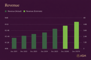 ASM has demonstrated the ability to withstand downturns (2023) while leveraging structural industry inflections (GAA, HBM) to outperform the broader market, supporting the thesis that its growth is driven by increasing ALD intensity rather than cyclical demand.
Margins
The progression of ASM’s margins is one of the strongest validations of its competitive positioning.
- 2023 gross margin: 48%
- 2024 gross margin: 50.5%
- 2025 gross margin: 51.8%
This steady expansion, alongside operating margin reaching a record 30.2% in 2025, reflects improved mix, increasing ALD intensity, higher service revenue, and ongoing efficiency programs.
Structurally, ASM operates in a precision bottleneck step within semiconductor manufacturing, enabling pricing power. Additionally, increasing layer counts at advanced nodes directly increase revenue per wafer, further supporting margin expansion.
Relative to peers, ASM’s margins sit at the upper end of the industry. Applied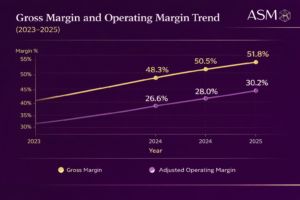 Materials (48–49%) and Lam Research (49–50%) operate slightly below ASM on gross margin, while Tokyo Electron represents the closest structural peer at the high end of the range.
Overall, ASM’s margin profile supports the view that its profitability is driven by technology and positioning rather than scale, reinforcing the durability of its competitive advantage.
R&D and Operating Discipline
To maintain its technological leadership, ASM continues to invest heavily in R&D while expanding margins.
- R&D: €470m in 2024 (+15%)
- R&D: €512m in 2025 (+9%)
R&D growth exceeded revenue growth in 2024, reflecting targeted investment at a key industry inflection point. In 2025, R&D growth moderated below revenue growth, indicating disciplined cost control alongside continued investment. SG&A remained tightly managed (+3% in 2024 and declining in 2025), supporting operating leverage expansion.
Peers also invest heavily in R&D (typically 11–13% of revenue), compared to ASM at 16–17%. While ASM’s absolute spend ($0.5bn) is lower than peers ($1.4–3bn), its investment is more concentrated and targeted, increasing effectiveness per euro spent.
This results in a model where ASM achieves profitability growth alongside sustained innovation, rather than at the expense of future competitiveness.
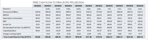
Free Cash Flow and Cash Conversion
ASM’s cash generation is strong and broadly tracks earnings growth:
- 2023 FCF: €447m
- 2024 FCF: €548m
- 2025 FCF: €615m
FCF margins improved from 17% in 2023 to 20% in 2025.
Cash conversion is high, supported by:
- limited capital intensity
- no structural working capital drag
- an asset-light model with outsourced manufacturing
- a growing high-margin services component
This has enabled consistent shareholder returns, including a dividend increase to €3.25 (c.15% 5-year CAGR) and ongoing €150m buyback programs.
Compared to peers, ASM’s FCF margins (19–20%) are below Applied Materials, Lam Research, and Tokyo Electron (22–30%). This reflects: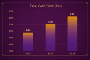
- higher R&D intensity
- continued growth-focused investment
- smaller scale
Despite this, cash flow quality remains high, with ASM self-funding growth, returning capital, and maintaining strategic flexibility.
Balance Sheet
ASM’s balance sheet is straightforward and highly conservative, with a net cash position and minimal leverage. This supports continued R&D investment,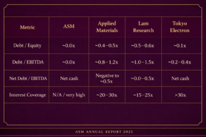 acquisitions, and shareholder returns without financial constraint.
Relative to peers, ASM operates at the most conservative end of an already financially disciplined industry, ensuring maximum flexibility across cycles.
Conclusion
Overall, ASM’s financials strongly support the strategic thesis. The company demonstrates consistent outperformance versus the WFE market, top-tier margins driven by technology rather than scale, disciplined but elevated R&D investment, and high-quality cash generation.
While free cash flow margins are modestly below peers, this reflects intentional reinvestment into structural growth opportunities, particularly in ALD and Epi. Combined with a conservative balance sheet, this positions ASM as a high-quality, structurally advantaged compounder, rather than a purely cyclical semiconductor equipment provider.
M&A Activity
ASM’s M&A Strategy
ASM’s M&A strategy is highly selective and differs from peers in the WFE industry, who are primarily focused on expanding across a broader range of process steps and using that scale to drive growth. ASM instead uses M&A to deepen its position within deposition and closely related technologies.
The company targets small to mid-sized, technology-driven businesses that enhance its capabilities in ALD and Epi. These acquisitions are typically bolt-on in nature rather than transformational, and are designed to integrate into ASM’s existing platform, reinforcing its niche leadership rather than pursuing broader market expansion.
In practice, this means ASM’s M&A activity is focused on:
- Strengthening its core deposition technologies
- Expanding into high-growth adjacencies such as silicon carbide and advanced packaging
- Enhancing internal capabilities through vertical integration or subsystem control
Key Transactions
LPE (Silicon Carbide Epitaxy) (2022)
The acquisition of LPE is ASM’s most strategically significant recent transaction, providing entry into the silicon carbide (SiC) epitaxy market. SiC is a high-growth segment driven primarily by power electronics applications.
From a strategic perspective, the transaction fits closely within ASM’s existing Epi capabilities while expanding its exposure beyond logic and memory into power semiconductors. Post-acquisition, the business has performed strongly, contributing meaningful revenue and enabling expansion of ASM’s customer base in both Europe and the US.
Reno Sub-Systems (RF / Plasma Technology) (2022)
This is a smaller-scale acquisition but is strategically important. Reno provides RF matching networks and generators, which are critical components in plasma-based processing tools.
This transaction represents a form of vertical integration, allowing ASM to improve control over key subsystems within its equipment. By integrating Reno’s technology, ASM can enhance tool performance, reliability, and process precision, all of which are critical in advanced semiconductor manufacturing.
Axus (Chemical Mechanical Planarization – CMP) (2025)
More recently, ASM has expanded into CMP through the acquisition of Axus, a provider of polishing equipment used in semiconductor manufacturing. CMP plays an important role in advanced packaging and 3D integration.
This transaction signals a measured expansion beyond pure deposition into adjacent process steps that are closely linked to interface engineering and materials performance, complementing ASM’s strengths in deposition and surface treatment.
However, this move also introduces a higher level of execution risk, as CMP is a more competitive and less concentrated market compared to ALD. As a result, the success of this acquisition will depend on ASM’s ability to differentiate technologically rather than compete on scale.
Value Creation Analysis
Across these transactions, ASM’s M&A activity can be evaluated across three key areas:
Strategic Fit
All major acquisitions align closely with ASM’s core competencies. LPE expands its Epi presence into a high-growth segment, Reno enhances internal capabilities within deposition tools, and Axus extends its reach into adjacent process steps. None of these deals represent a deviation from the company’s core focus on materials engineering and atomic-scale processing.
Synergies
The primary synergies are revenue and technology-driven rather than cost-driven. ASM is able to leverage its existing customer relationships to scale acquired technologies, while also integrating new capabilities into its broader product portfolio. Operational synergies, such as supply chain and manufacturing scale, further support margin expansion.
Financial Quality
While ASM does not rely heavily on M&A for growth, its acquisitions have generally contributed positively to revenue and strategic positioning. The company’s strong free cash flow generation allows it to pursue these opportunities without compromising financial flexibility, and there is no evidence of aggressive or value-destructive deal-making.
Conclusion
Overall, M&A is not a primary growth driver for ASM International, but rather a targeted tool used to strengthen its competitive positioning. The company’s acquisitions are highly selective, technologically aligned, and focused on reinforcing its leadership in deposition and materials engineering.
This disciplined approach allows ASM to expand into attractive adjacencies while maintaining strategic focus, supporting long-term value creation without introducing significant execution risk.
Key Risks
ASM is positioned for structural growth via increasing ALD intensity. However, revenue, margins, and valuation remain dependent on the timing of node transitions, customer capital expenditure cycles, and the extent to which expected increases in deposition intensity fully materialise in practice.
Risk 1: WFE Cyclicality / Capex Volatility
Semiconductor capital expenditure is inherently volatile, driving swings in ASM’s revenue. The business remains directly linked to tool shipments, meaning customer delays or reductions in orders have an immediate impact on revenue.
This was clearly demonstrated in 2023, where a collapse in memory capex led to a 40% decline in ASM’s memory sales, alongside a mid-teens contraction in the broader WFE market. These cycles do not only affect near-term revenue, but also feed through to node timing, with delays in fab ramps pushing out demand for ALD tools.
Mitigating factors include the growth of higher-margin, recurring services revenue (19% CAGR), increasing ALD intensity per device providing a structural offset, and ASM’s exposure to leading-edge logic, which typically recovers earlier in the cycle.
Overall, while ASM is structurally less cyclical than peers, it remains directionally exposed to semiconductor capex cycles.
Risk 2: Customer Concentration, Node Timing & Technology Adoption
ASM’s growth is dependent on a small number of customers ramping advanced nodes on schedule. In practice, leading-edge spending is concentrated among TSMC, Samsung, and Intel, making ASM’s growth closely tied to their capital allocation and execution.
Historically, node transitions have not been linear. The transition to GAA saw a gradual progression from pilot lines to volume manufacturing across 2024–2025, while in 2023, fab delays led to order pushouts. These timing effects directly translate into fewer tools being shipped and lower near-term demand.
More subtly, ASM’s growth also depends on the degree to which expected increases in ALD and Epi intensity actually materialise. If new materials, layers, or process steps are adopted more slowly than expected, the expansion in ASM’s served available market may fall short of projections.
While diversification into memory and services provides some offset, ASM remains fundamentally dependent on the timing, scale, and technical execution of a small number of leading-edge customers.
Risk 3: China Normalisation / Export Controls
China has been a major swing factor for ASM, both in terms of demand and regulatory exposure. At peak, China accounted for more than 30% of revenue, supporting growth through 2023 and 2024, before beginning to normalise in 2025. Export controls have also been an explicit company risk factor across prior reporting periods.
Export controls represent a clear regulatory risk, with prior guidance indicating a potential 15–25% impact on sales in affected segments. At the same time, demand in China is inherently volatile, reflecting periods of heavy investment followed by digestion.
This creates multiple transmission channels: regulatory restrictions can limit shipments, while demand normalisation following overinvestment can reduce order volumes. In addition, a shift away from China may negatively impact margins if revenue mix moves toward lower-margin regions.
While ASM benefits from global demand, particularly driven by AI-related investment, China remains a structurally more volatile component of the revenue base.
Risk 4: Competitive Pressure
The WFE market is highly competitive, and ASM faces the risk of losing market share or pricing power in ALD and Epi.
Although ASM holds an estimated 55% share in ALD, this leadership must be maintained through successive technology nodes. Competitors such as Applied Materials, Tokyo Electron, and Lam Research have significantly larger R&D budgets and broader process integration capabilities, allowing them to compete across multiple parts of the process flow.
Loss of tool-of-record positions at advanced nodes would directly impact revenue, while increased competition could lead to pricing pressure and margin compression.
However, this risk is mitigated by high switching costs, deep customer integration, and long qualification cycles. As a result, ASM’s leadership position appears durable, though not monopolistic.
Risk 5: Power / SiC Weakness
Non-core segments, particularly silicon carbide (SiC) and broader power/analog markets, present a secondary risk through their potential to drag on growth.
These markets have been weak across 2024 and 2025, driven by slower electric vehicle demand and prior overcapacity. This has resulted in reduced demand for related tools, limiting ASM’s diversification benefits.
While these segments represent a minority of total revenue and do not underpin the core investment thesis, prolonged weakness can weigh on near-term performance and reduce earnings support outside of leading-edge logic and memory.
Conclusion
Overall, the primary risks to ASM are not centred on the long-term relevance of its technology, but on the timing, magnitude, and realisation of its growth drivers. The company remains exposed to semiconductor capex cycles, concentrated customer spending, and the execution of key technology transitions. While structural trends such as increasing ALD intensity provide a strong foundation for long-term growth, variability in node timing, regional demand, and competitive dynamics can lead to meaningful deviations in near-term performance.
Valuation and Performance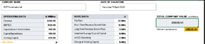
Assumptions
Revenue growth is assumed at 12% in the near term, reflecting continued momentum from the transition to gate-all-around (GAA) architectures, increasing ALD intensity, and strong demand across advanced logic and memory. Growth is gradually tapered over the forecast period to reflect normalization of semiconductor capital expenditure cycles, converging toward a long-term growth rate of 3.5%. This terminal rate is broadly aligned with long-term semiconductor demand, with a modest premium to GDP reflecting ASM’s structural positioning within deposition.
Operating margins are assumed to remain strong, supported by a favourable product mix and operating leverage as the company scales. Capital intensity remains moderate, with capital expenditure slightly above depreciation, consistent with continued investment in R&D and capacity expansion.
Working capital investment is modelled at approximately 5% of incremental revenue. While current working capital represents 10% of revenue, the forward assumption reflects improving efficiency, customer prepayments, and a growing contribution from less working-capital-intensive services.
A weighted average cost of capital (WACC) of 8% is applied, reflecting ASM’s strong margins, asset-light model, and structural growth profile, while still incorporating the inherent cyclicality of the semiconductor equipment industry.
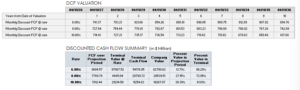
Valuation Output
Under these assumptions, the model implies an enterprise value of approximately €28.5bn. This compares to a market capitalisation of approximately €37.0bn as of April 11th, implying c.23% downside based on base-case assumptions.
Relative DCF Comparison
To provide context, similar DCF frameworks applied across key peers indicate a broader disconnect between intrinsic value and current market pricing. Lam Research screens at 57% implied overvaluation, Applied Materials at 51%, and Tokyo Electron at 40%.
Compared to these peers, ASM screens as less stretched on a DCF basis, with a materially smaller implied downside. This suggests that while ASM is trading above intrinsic value under conservative assumptions, the degree of premium is more moderate relative to the broader semiconductor equipment sector.
Interpretation
The consistent pattern of DCF-implied overvaluation across the peer group suggests that current market valuations are being driven by a sector-wide re-rating rather than company-specific mispricing. This re-rating is likely supported by expectations of sustained AI-driven demand, increasing semiconductor capital intensity, and structural growth in advanced node technologies.
In ASM’s case, the valuation premium appears to reflect market confidence in its leading position in ALD and its leverage to key structural drivers such as GAA adoption and increasing materials intensity. However, the base-case DCF suggests that a significant portion of this upside is already reflected in the current share price. Sensitivity analysis indicates that valuation is particularly responsive to WACC and terminal growth assumptions, with modest changes bringing the implied valuation closer to current market levels.
Conclusion
Overall, the DCF suggests that ASM is fully valued to modestly overvalued under conservative assumptions, with current pricing implying a more optimistic outlook for long-term growth and sector dynamics. Relative to peers, ASM appears less overextended, supporting the view that its premium valuation is at least partially justified by its structural positioning within the semiconductor equipment industry.
Other Valuation Metrics
To complement the DCF analysis, ASM is compared against key semiconductor equipment peers including Applied Materials, Lam Research, and Tokyo Electron across a range of valuation multiples.
On a forward P/E basis, ASM trades at 33.6x, broadly in line with Applied Materials (32.3x), below Lam Research (43.0x), and broadly comparable to Tokyo Electron (35–36x), suggesting no meaningful earnings premium despite stronger structural growth.
On an EV/EBITDA basis, ASM trades at 22.4x versus 27.3x for Applied Materials, 35.1x for Lam Research, and 25.7x for Tokyo Electron, indicating a clear discount despite strong margins and profitability.
On an EV/Sales basis, ASM trades at 8.3x, below Applied Materials (9.0x) and Lam Research (12.7x), but slightly above Tokyo Electron (7.2x), placing it in the middle of the peer range despite its exposure to higher-growth ALD segments.
On a price-to-book basis, ASM trades at 7.7x, below Applied Materials (13.1x), Lam Research (28.2x), and Tokyo Electron (8.9x), reflecting its asset-light model but reinforcing that valuation is not driven by balance sheet strength.
Overall, ASM does not screen as expensive relative to peers and in several cases
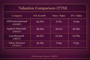
trades at a discount, particularly on EV/EBITDA. When combined with the DCF, which suggests c.20–25% downside, this indicates that while ASM’s relative valuation is justified, absolute sector valuations appear elevated, with the market pricing a more optimistic scenario around sustained growth, AI-driven demand, and ALD intensity than reflected in base-case assumptions.
Share Performance
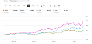
Over the past year, ASM International has delivered a return of approximately 103%, outperforming Tokyo Electron (94%) but lagging Applied Materials (174%) and significantly underperforming Lam Research (294%). This suggests that while ASM has participated in the broader semiconductor upcycle, it has not been the primary beneficiary of recent multiple expansion within the sector.
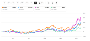
Over a five-year period, ASM has returned approximately 175%, broadly in line with Applied Materials (193%) but below Lam Research (314%), while significantly outperforming Tokyo Electron (80%). This reflects strong long-term value creation, although not to the same extent as the highest-beta names in the sector.
Overall, ASM’s performance indicates consistent participation in the semiconductor cycle, but with less aggressive multiple expansion than peers such as Lam Research, supporting the view that its valuation has been comparatively more disciplined despite strong underlying fundamentals.
Final Conclusion
ASM International stands out not as a broad semiconductor equipment supplier, but as a highly specialised operator concentrated in one of the most important and economically attractive areas of wafer fabrication: advanced deposition. That positioning matters. As semiconductor progress becomes increasingly dependent on materials engineering, 3D architectures, and atomic-level process control, the number, complexity, and value of ALD and Epi steps continues to rise. This creates a structural tailwind that is stronger and more durable than simple semiconductor unit growth.
Across the report, the same conclusion keeps reappearing from different angles. The industry structure is attractive, ASM’s niche within it is even more attractive, and the company’s execution has so far validated the thesis. It has outgrown the broader WFE market, expanded margins, maintained leadership in ALD, improved its Epi position, and continued to invest heavily in R&D without compromising balance-sheet strength. The company is therefore best understood not as a generic cyclical equipment name, but as a structurally advantaged compounder operating inside a cyclical industry.
That said, the investment case is not without tension. Near-term outcomes remain sensitive to node timing, customer capex, China demand, export controls, and the pace at which technology inflections fully materialise. In addition, valuation already reflects a meaningful portion of the long-term optimism. So while the quality of the business is clear, the debate increasingly shifts from whether ASM is a strong company to how much of that strength is already priced in.
Overall, ASM appears to be one of the best-positioned companies in semiconductor equipment for the next phase of industry evolution. Its exposure to GAA, HBM/DRAM, structural ALD intensity growth, Epi share gains, and services expansion gives it multiple paths to continued outperformance. If the core technology transitions play out as expected, ASM should remain levered to some of the highest-growth, highest-value, and hardest-to-replicate parts of semiconductor manufacturing over the coming years.
- Author: Craig Evans
References & Resources
Company Filings and Investor Materials
- ASM International – Annual Reports (2022–2025)
- ASM International – Investor Day 2025 Presentation
- Lam Research – Form 10-K (2024, 2025)
- Tokyo Electron – Integrated Reports (2024, 2025)
Industry Reports and Market Research
- Global Atomic Layer Deposition (ALD) Market Report – LinkedIn Article
https://www.linkedin.com/pulse/global-atomic-layer-deposition-ald-coating-systems-0ntcc/ - Wafer Fab Equipment Market Report – Cognitive Market Research
https://www.cognitivemarketresearch.com/wafer-fab-equipment-market-report - World Semiconductor Trade Statistics – Semiconductor market data and long-term forecasts
- TechInsights – Industry share data and process-level insights (as referenced in company materials)
Peer Benchmarking and Financial Data
- Applied Materials – Investor Relations and Financial Filings
- Lam Research – Investor Relations and Financial Filings
- Tokyo Electron – Investor Relations and Financial Filings
- Seeking Alpha – Peer comparison data and valuation tables
Leave a Reply